
Metrology Process Engineer (CD-SEM) at Intel Corporation
Intel Corporation, Hillsboro, USA. | Nov, 2021 - July, 2025
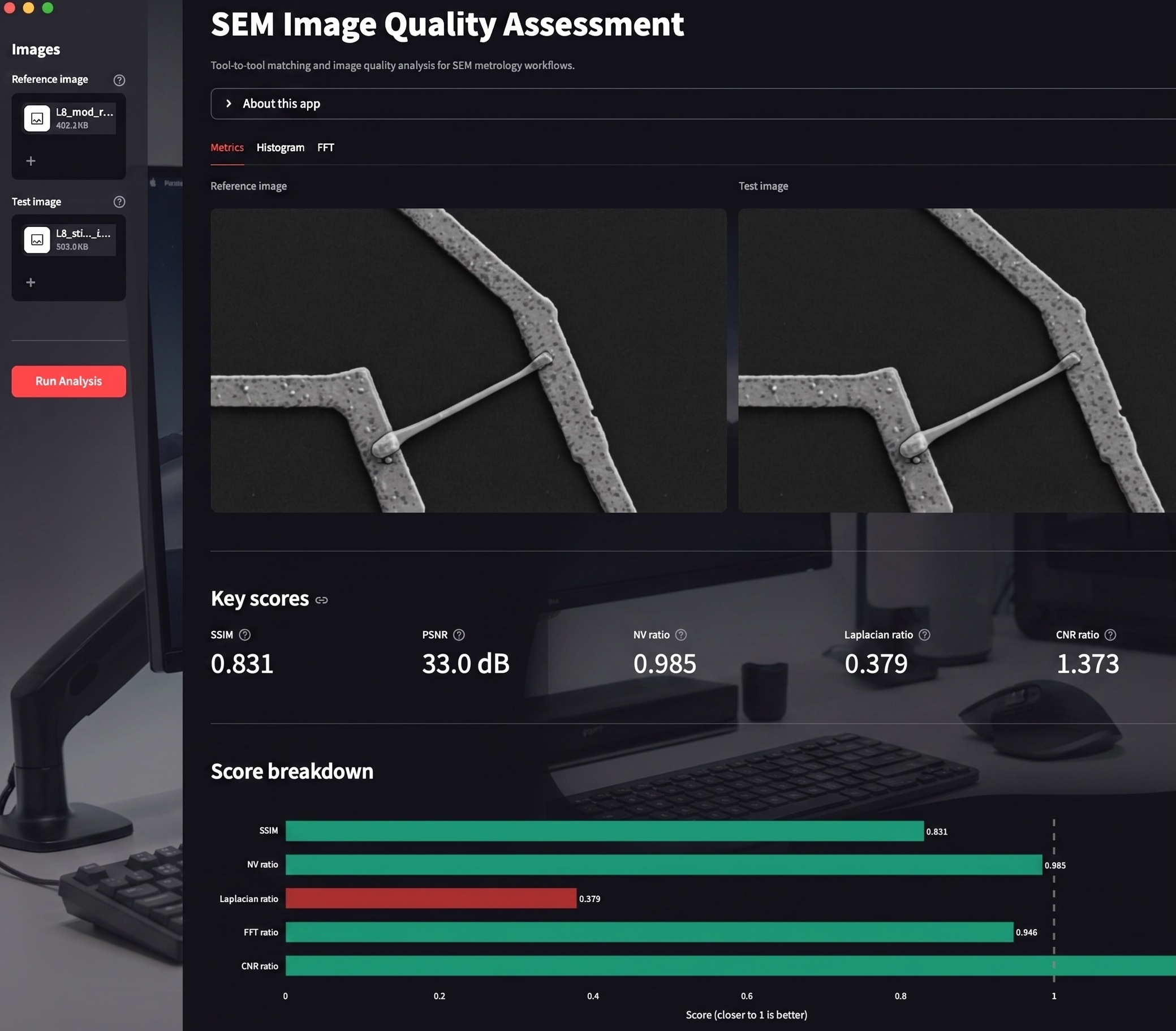
- Developed and deployed a Python-based image quality analysis pipeline applying multiple IQA algorithms (sharpness, CNR, FFT high-frequency energy, GLCM) to characterize SEM imaging sensor performance and resolve a recurring measurement drift issue that had been managed reactively for over 3–4 years — transitioning a team of 5 engineers from reactive troubleshooting to proactive, data-driven maintenance.
- Managed fleet-wide gauge capability and measurement stability through SPC, automated calibration logic, and GR&R studies to sustain Cp/Cpk targets and minimize measurement drift across advanced process nodes.
- Independently developed and deployed the workgroup's first long-term SPC trend monitoring pipeline using SQLPathfinder and Python — enabling fleet-wide longitudinal visibility into metrology performance and cutting data processing time by 80%.
- Performed structured root cause investigations on electron-optical drift and imaging anomalies; coordinated corrective actions across hardware, software, and process integration teams.
Owned imaging system performance, sensor analytics, and measurement stability for advanced CD-SEM metrology equipment in high-volume semiconductor manufacturing. Drove cross-functional engineering investigations spanning hardware, software, and process integration to improve fleet-wide gauge capability, reduce measurement drift, and shift the team from reactive troubleshooting toward data-driven, proactive maintenance.
Graduate Research Scholar
University of California, Merced, California. | Aug, 2016 - Oct, 2021
PhD research at the intersection of optical physics, computational electromagnetics, and experimental metrology — focused on light–matter interactions in plasmonic nano-structures and nanoscale energy transfer.
Computational Modeling of Plasmonic Metastructures- Developed a hybrid full-wave electromagnetic modeling framework combining the Method of Fundamental Solutions (MFS) and Foldy–Lax multiple-scattering theory to simulate scattering from dielectric cores coated with plasmonic nanoparticle assemblies.
- Implemented Python and MATLAB solvers to compute far-field scattering, extinction spectra, anisotropy, and albedo across large parameter spaces; identified regimes of scattering suppression, angular redistribution, and broadband cloaking.
- Nano-fabricated core–shell plasmonic structures and validated simulation predictions against experimental scattering measurements, with strong agreement across visible and near-IR wavelengths.
- Published in JOSA A and Optics Express; foundational to my current interest in surrogate modeling, physics-informed learning, and data-driven methods for imaging and wave-based systems.
- Designed, built, and qualified a custom high-stability TRPL optical measurement system optimized for dilute samples and weak emitters; defined specifications, aligned optical components, and developed calibration protocols.
- Probed non-radiative energy transfer in DNA-templated gold nanoclusters using time-resolved photoluminescence to distinguish FRET-type from NSET-type transfer mechanisms across 5–17 nm separations.
- Mentored undergraduate researchers and contributed data to multiple CCBM projects.
Graduate Research Associate
Universal Instruments Corporation, Conklin, New York. | 2013-2014
- Characterized thermomechanical properties of lead-tin-silver alloys for high-temperature electronic packaging.
- Conducted DSC analysis to determine melting point depression and thermodynamic behavior.
- Performed SEM-based microstructural analysis to link material composition with grain morphology.
- Measured mechanical integrity using a Dage 4000 Plus bond tester and co-authored an IMAPS industry publication.
- Co-authored an industry-facing publication for the International Microelectronics Assembly and Packaging Society (IMAPS), presenting findings to aid in the development of new industrial alloys.
Ph.D., Physics (Optics | Computational Modeling | Nano fabrication)
Aug 2016 to Oct 2021 | University of California, Merced.
M.S., Physics
2016 | Binghamton University (SUNY) , Binghamton, NY.
- Khan, M.I., et al., “Scattering by nanoplasmonic mesoscale assemblies,” JOSA A 42, 1244–1253 (2025).
- Khan, M.I., et al., “Modeling broadband cloaking using 3D nano-assembled plasmonic meta-structures”, Optics Express, 2020.
- Khan, M.I., et al., “Effect of Sn Component Surface Finish on 92.5 Pb-5Sn-2.5 Ag”, HITEC, 2014.
- Khan, M.I., et al., “Collective motion in heterogeneous drone swarms”, APS March Meeting 2018, abstract id.S51.013.